Skip To Content

J-Lead Forming of a MOSFET Transistor for the Military Industry

J-Lead Forming of a MOSFET Transistor for the Military Industry

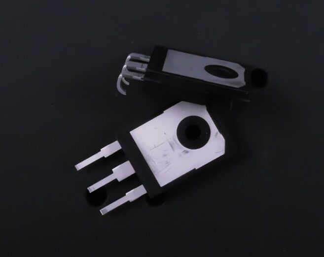
Tintronics completed the J-lead Forming of a MOSFET transistor, which is used in a high-efficiency switching application for a military client. The company employed a custom-designed forming die, a bench-top lead form press and a manual hot solder dip station. The parts meet tight tolerances of .161” ±.010” from the lead exit to the inside bend and .050” ±.030” on the radius. The primary processes, lead forming and tinning, and the secondary processes, lead scanning and visual and final inspections, ensured the parts met the customer-supplied specifications as well as the IPC J-STD-001, IPC/JEDEC J-STD-033B.1 and ANSI/ESD S20.20 standards. The production runs were low-volume.

Project Highlights for this MOSFET Transistor for the Military

Product Description This MOSFET transistor is used within a high
efficiency switching application
Capabilities Applied/Processes Primary:
Lead Forming
Tinning
Secondary:
Lead Scanning
Inspection
Equipment Used to Manufacture Part Custom designed forming die
Benchtop lead form press
Manual hot solder dip station
Package Style TO-247
Tightest TolerancesLead exit to inside bend .161 ±.010
Radius .050 ±.030
Material of LeadsPlated copper alloy
Material UsedSn63 Pb37 solder
In process testing performedVisual Inspection
Final Inspection
Industry for UseDefense
QuantityLow volume
Standards MetCustomer supplied specifications
IPC J-STD-001
IPC/JEDEC J-STD-033
ANSI/ESD S20.20
Project NameJ-Lead Forming of MOSFET Transistor